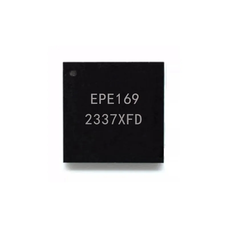
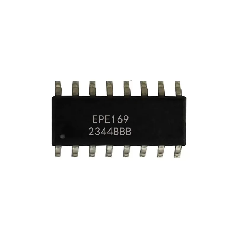
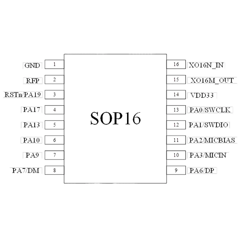
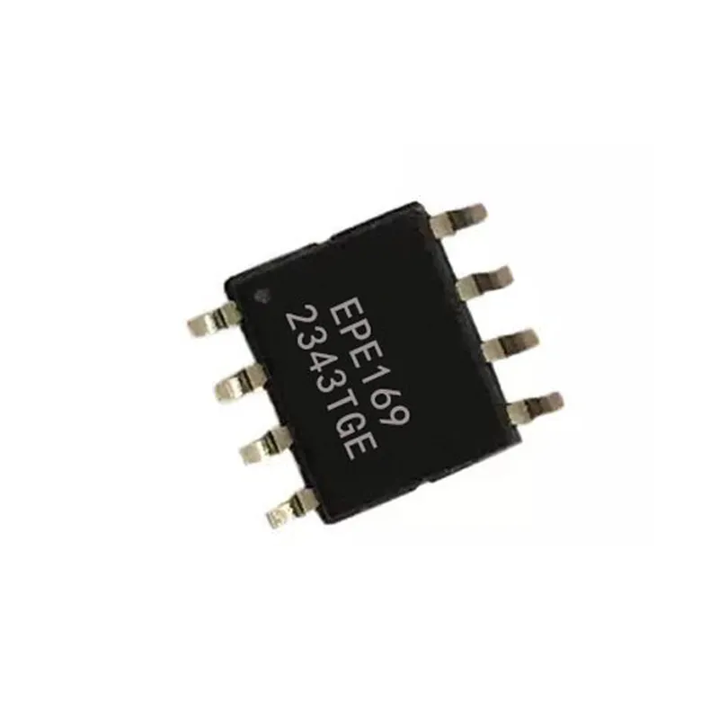
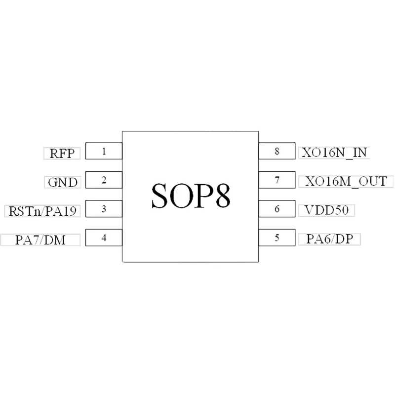
| Bluetooth BT 5.2 + 2.4GHz (proprietary protocol) SoC |
Supports BLE data rates: 1 Mbps, 2 Mbps |
| Sensitivity: -96 dBm at 1 Mbps BLE mode |
| Sensitivity: -92 dBm at 2 Mbps BLE mode |
| Transmit power: -40 dBm to 6 dBm |
| Single-ended antenna output |
| Integrated balun |
| Supports BLE Mesh |
| 32-bit RISC MCU |
High-performance (64MHz) |
| SMART 8-channel DMA controller |
| CACHE Support Scope |
4KB |
| USB |
USB 1.1 full-speed operation at 12 Mbps |
| Supports up to 5 endpoints; endpoints 1–4 support simultaneous transmit and receive |
| FIFO depth for all endpoints is 64 bytes |
| On-chip memory |
4KB ROM |
| Up to 32 KB of SRAM |
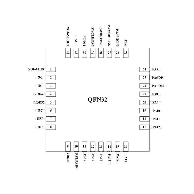
| SOP32(SIP 256KB QSPI FLASH) |
| Clock source |
Supports 16MHz crystal oscillator (XTAL) |
| Internal high-frequency RC oscillator (IRC): 16MHz ±2% |
| Ultra-low-power internal low-frequency RC oscillator (RC32K) |
| Internal high-frequency DPLL (48MHz/64MHz) clock |
| Supports external clock input |
| System clock (RTC) |
Operates using ultra-low-power technology |
| Driven by an internal ultra-low-power RC oscillator |
| Watchdog Timer |
Operated by an internal low-power WDT |
| Counter/Timer Modules |
1 x Advanced 16-bit Counter/Timer (ATMR) |
| 1 x Common 16-bit Counter/Timer (CTMR) |
| Supports 4 independent channels for input capture, output compare, and PWM |
| 1 x Basic 16-bit Counter/Timer (BTMR) |
| Peripheral Interfaces |
2 x UART, supporting RS485/IrDA/ISO7816-3, with data rates up to 3.84 Mbps |
| 1 SPI Master interface, with a maximum speed of up to 16 Mbps |
| 1 SPI Slave interface, with a maximum speed of up to 16 Mbps |
| 1 x I2C bus, configurable as master/slave, supporting Fast Mode with data rates up to 400 Kbps |
| Analog-to-Digital Converter (ADC) |
10-bit resolution, 1 Mbps ADC, 10 input channels |
| Voice functionality, supporting 8K sampling rate |
| General-Purpose I/O (GPIO) |
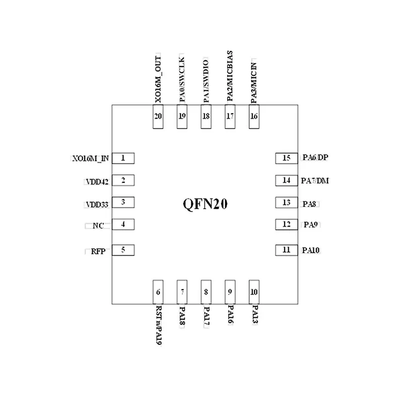
Supports up to 20 GPIOs; each I/O supports interrupt and wake-up functions. |
| Power Management Unit (PMU) |
Integrated Power-On-Reset (POR) |
| Integrated Low-Voltage-Detect (LVD) with a default voltage threshold of 1.65V. |
| Voltage Range |
Operating voltage: 1.8V – 4.3V (determined by the specific chip model). |
| Current Consumption |
On-chip LDO voltage regulator |
| 44.7 µA/MHz (@3.3V with 16 MHz RC oscillator) |
| Deep sleep mode: 70 µA @3.3V |
| Power-off mode: 2 µA @3.3V |
| BLE/2.4G mode: Tx peak current 7.2 mA (@1.8V, 0 dBm) |
| BLE/2.4G mode: Rx peak current 10.3 mA (@1.8V) |
| ESD 4500V |
| Operating temperature -40°C to 105°C |